
Ask questions which are clear, concise and easy to understand.
Ask QuestionPosted by Anuradha Patwari 5 years, 3 months ago
- 3 answers
Preeti Yadav 5 years, 2 months ago
Posted by Gungun Gupta?? 5 years, 3 months ago
- 4 answers
Posted by Atul Misha 5 years, 3 months ago
- 1 answers
Student Of The Year 5 years, 3 months ago
Posted by Muddabbir Hussain 5 years, 3 months ago
- 1 answers
Saloni Kaushik 5 years, 2 months ago
Posted by Nishu Singh 5 years, 3 months ago
- 1 answers
Divyanshi Gupta 5 years, 3 months ago
Posted by Akansha Chaudhry 5 years, 3 months ago
- 0 answers
Posted by Mr. Singh 5 years, 3 months ago
- 1 answers
Gaurav Seth 5 years, 3 months ago
When an inductor and capacitor are connected together , energy flows from capacitor to inductor and then back to capacitor. This process continues forever in the absence of resistance in a cyclic oscillatory manner. Since there is no resistance, energy can not dissipate via inductor and capacitor and the whole energy of the system continues to swing back and forth between inductor and capacitor.
Let a capacitor which is initially charged as Q₀ and an inductor with initial current 0 are connected together.
So the initial energy of the system,
U₀ = energy stored in the capacitor + energy stored in the inductor
= Q₀²/2C + 0
= Q₀²/2C
when the switch is closed current starts flowing in the circuit and capacitor starts discharging, this current flows in the circuit until the capacitor is discharged completely. Let the final maximum current be I₀.
So final energy stored in the system now
Uₙ = energy stored in the capacitor + energy stored in the inductor
= 0 + LI₀²/2
= LI₀²/2
This current continues to flow in the circuit even after the capacitor is discharged totally because the inductor opposes the change in current. So this current now starts charging the capacitor until it is fully charged in the reverse polarity. This cycle of energy flow continues forever.
At any point the energy stored in the system will be the sum of energy stored in the capacitor and inductor.
U = Q²/2C + LI²/2
Since there is no resistance in the circuit energy dissipation does not takes place and the total energy of the system always remains constant.
Hence ,
U = Q²/2C + LI²/2 = LI₀²/2 = Q₀²/2C
Posted by Mr. Singh 5 years, 3 months ago
- 1 answers
Gaurav Seth 5 years, 3 months ago
A pure inductor of 25mh is connected to a source of 220v.Find inductive reactance and rms current in the circuit, frequency of source is 50Hz. |
|
Inductance of Inductor, L = 25 m H = 2 x 3.14 x 50 x 25 x 10-3 = 7.85 ?
|
 Inductive reactance , XL = 2? f L
Posted by Sreelakshmi Sree 5 years, 3 months ago
- 1 answers
Gaurav Seth 5 years, 3 months ago
Transparent medium is denser medium as compared yo air bubble,as we know whenever light travels from a denser medium to rared medium it bends aways from normal,hence air bubble inside a transparent medim behaves like a diverging lens as it diverges the rays(moves away from normal).
Posted by Gungun Gupta?? 5 years, 3 months ago
- 5 answers
Lax Chauhan 5 years, 3 months ago
Posted by Gungun Gupta?? 5 years, 3 months ago
- 4 answers
Tanya ?? 5 years, 3 months ago
Posted by Krishna Rathore 5 years, 3 months ago
- 2 answers
Raj Choudhary 5 years, 3 months ago
Posted by Student Of The Year 5 years, 3 months ago
- 5 answers
Posted by Yogeshwar Singh Rathore 5 years, 3 months ago
- 1 answers
Meghna Thapar 5 years, 3 months ago
Insulating material - a material that reduces or prevents the transmission of heat or sound or electricity. insulant, insulation. building material - material used for constructing buildings. lagging - used to wrap around pipes or boilers or laid in attics to prevent loss of heat. Insulation enhances the thermal performance of the building envelope by reducing heat gain in hot weather and heat loss in cold weather thereby limiting the need for cooling and heating. However, conventional insulation materials have high embodied energy values.
Posted by Anuradha Patwari 5 years, 3 months ago
- 1 answers
Student Of The Year 5 years, 3 months ago
Posted by Preeti Yadav 5 years, 3 months ago
- 5 answers
Shivansh Kaushik 5 years, 3 months ago
Muddabbir Hussain 5 years, 3 months ago
Posted by Mohd Arshad 5 years, 3 months ago
- 1 answers
Meghna Thapar 5 years, 3 months ago
Gauss’s Theorem Statement:
According to Gauss’s theorem the net-outward normal electric flux through any closed surface of any shape is equivalent to 1/ε0 times the total amount of charge contained within that surface.
Proof of Gauss’s Theorem Statement:
Let the charge be = q
Let us construct the Gaussian sphere of radius = r
Now, Consider , A surface or area ds having having ds (vector)
Normal having the flux at ds:
Flux at ds:
d e = E (vector) d s (vector) cos θ
But , θ = 0
Therefore, Total flux:
C = f d Φ
E 4 π r2
Therefore,
σ = 1 / 4πɛo q / r2 × 4π r2
σ = q / ɛo
Posted by Mohd Arshad 5 years, 3 months ago
- 1 answers
Gaurav Seth 5 years, 3 months ago
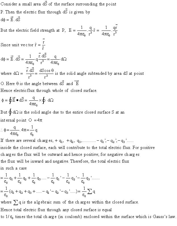
Statement of Gauss"s Theorem : The net-outward normal electric flux through any closed surface of any shape is equal to
1/ε0 times the total charge contained within that surface , i.e.,

over the whole of the closed surface, q is the algebraic sum of all the charges (i.e., net charge in coulombs) enclosed by surface S.

Proof of Gauss"s Theorem :
Let a point charge +q coulomb be placed at O within the closed surface. Let E be the electric field strength at P. Let
OP= r and the permittivity of free space or vaccuum be ε0.
 </article>
Posted by Tanisha Shrivastava 5 years, 3 months ago
- 2 answers
Yogita Ingle 5 years, 3 months ago
Refractive index of diamond is 2.42 and the critical angle is 24.40 only. The faces of diamond are cut in such a way that a ray of light entering the diamond suffers repeated total internal reflections (angle of incidence is greater than the critical angle) at different faces and remains confined within the diamond. Thus it sparkles.
Posted by Sarika Singh 5 years, 3 months ago
- 0 answers
Posted by Harshini S 5 years, 3 months ago
- 1 answers
Gaurav Seth 5 years, 3 months ago
Depends on you, and your level of preparation by now. Whatever may it be, you can do much much more as 2 months are good enough for CBSE.
1. For Physics, focus on NCERTs and past year papers. Derivations are crucial low hanging fruits. Churn them out from scratch, as if you’re explaining it to someone else. Don’t miss a step. Read, understand, and write till you can derive the equations/theorems from scratch.
2. For Chemistry, Focus only and only on NCERTs. For chapters like surface chemistry, p-block, polymers, everyday life and stuff like that, you really need to know the chapter to its utmost details. There must not be a single line which you miss out while studying. Yet, some parts would require knowing which is not in NCERTs, like in the chapter of Solid State, structures of ionic compounds is not given in detail (rock salt, zinc blende); yet, CBSE has asked it many times. So, past year papers are of great help to practice. Also making notes for chemistry is extremely helpful, and I cannot stress this more. I scored 100/100 in Chemistry, and I hope this adds some credibility to my answer.
3. For Maths, you need to know beyond the NCERTs to score well. R.D Sharma is more than sufficient. But, just don’t entangle yourself into the huge collection of problems in R.D Sharma. You need to respect the fact that you’ve woken up quite late. There’s absolutely no time to master each and every concept. Focus on practicing the solved examples. That would do. Also, don't forget the past year papers.
Posted by Rajat Yadav 5 years, 3 months ago
- 3 answers
Aaryan Verma 5 years, 3 months ago
Yogita Ingle 5 years, 3 months ago
| Sl No | P-type Semi conductor | N-type semi conductor |
| 1 | P-type semiconductor is formed due to the dopping of III group elements i.e. Boron, Aluminium, Thallium. | N-type semi conductor is formed due to dopping of Nitrogen, Phosporus, Arsenic, Antimony, Bismoth. |
| 2 | These are also known as Trivalent semi conductors. | These are also known pentavalent semiconductor. |
| 3 | P-type semiconductors is positive type semiconductor it means it deficiency of 1 electron is required. | N-type semiconductor is negative type semi-conductor it means excess of 1 electron is required. |
| 4 | In P-type semiconductor majority charge carries are holes and minority charge carries are electrons. | In N-type semiconductor majority charge carries are electrons and minority charge carries are hole. |
| 5 | A hole indicates a missing electron. In this no. of holes is more than the no. of electrons. | In N-type semiconductor the no. of holes is less than the no. of free electron. |
Avinash Mathuri 5 years, 3 months ago
Posted by Rajat Yadav 5 years, 3 months ago
- 1 answers
Yogita Ingle 5 years, 3 months ago
| Intrinsic Semiconductor | Extrinsic Semiconductor |
| Pure type of semiconductor | Impure type of semiconductor |
| Density of electrons is equal to the density of holes | Density of electrons is not equal to the density of holes |
| Electrical conductivity is low | Electrical conductivity is high |
| Dependence on temperature only | Dependence on temperature as well as on the amount of impurity |
| The bandgap between conduction (C.B) and valence band (V.B) is small. | The energy gap is higher than the intrinsic semiconductors. |
| Examples: Si, Ge | Examples: GaAs, GaP |
Posted by Arif Khan 5 years, 3 months ago
- 1 answers
Posted by Anuradha Patwari 5 years, 3 months ago
- 2 answers
Posted by Rohit Raj 5 years, 3 months ago
- 1 answers
Posted by Mr. Singh 5 years, 3 months ago
- 0 answers

myCBSEguide
Trusted by 1 Crore+ Students

Test Generator
Create papers online. It's FREE.
![]()
CUET Mock Tests
75,000+ questions to practice only on myCBSEguide app

Muddabbir Hussain 5 years, 3 months ago
5Thank You