Extra Questions for Class 12 Physics Electronic Devices. We know Physics is tough subject within the consortium of science subjects physics is an important subject. But if you want to make career in these fields like IT Consultant, Lab Technician, Laser Engineer, Optical Engineer etc. You need to have strong fundamentals in physics to crack the exam. myCBSEguide has just released Chapter Wise Question Answers for class 12 Physics. There chapter wise Extra Questions with complete solutions are available for download in myCBSEguide website and mobile app. These Questions with solution are prepared by our team of expert teachers who are teaching grade in CBSE schools for years. There are around 4-5 set of solved Physics Extra Questions from each and every chapter. The students will not miss any concept in these Chapter wise question that are specially designed to tackle Board Exam. We have taken care of every single concept given in CBSE Class 12 Physics syllabus and questions are framed as per the latest marking scheme and blue print issued by CBSE for class 12.
Class 12 Physics Extra Questions
Practice Questions of Class 12 Physics Chapter 14
Class – 12 Physics (Electronic Devices)
-
The output from a full wave rectifier is
- a pulsating unidirectional voltage
- a dc voltage
- zero
- unidirectional voltage having ripples
-
In a pure, or intrinsic, semiconductor, valence band holes and conduction-band electrons are always present
- None of these
- such that number of holes is greater than the number of electrons
- in equal numbers
- such that number of electrons is greater than the number of holes
-
When Ge crystal is doped with phosphorus atoms, it becomes
- superconductor
- Insulator
- n-type
- p-type
-
In n-type semiconductor the total number of conduction electrons {tex}{{\rm{n}}_{\rm{e}}}{/tex} is due to the,
- holes generated intrinsically only
- electrons generated intrinsically only
- electrons contributed by donors and those generated intrinsically
- holes contributed by donors and those generated intrinsically
-
In an unbiased p-n junction, holes diffuse from the p-region to n-region because:
- all of these
- they move across the junction by the potential difference.
- hole concentration in p-region is more as compared to n-region.
- free electrons in the n-region attract them.
-
State the relation between the frequency {tex}\nu{/tex} of radiation emitted by LED and the band gap energy E of the semiconductor used to fabricate it.
-
What is the most common use of photodiode?
-
What happens to the width of depletion layer of a p-n junction when it is
- forward biased?
- reverse biased?
-
Draw energy band diagram of n-type and p-type semiconductor at temperature T > OK. Mark the donar and acceptor energy level with their energies.
-
Draw and explain the output waveform across the load resistor R, if the input waveform is as shown in the given figure.

-
State the factor, which controls:
- Wavelength of light and
- intensity of light emitted by an LED.
-
Explain, with the help of a circuit diagram, how the thickness of depletion layer in a p-n junction diode changes when it is forward biased. In the following circuits which one of the two diodes is forward biased and which is reverse biased?


-
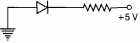
- In the following diagram, is the junction diode forward biased or reverse biased?
- Draw the circuit diagram of a full wave rectifier and state how it works?
- In the following diagram, is the junction diode forward biased or reverse biased?
-
- Why are Si and GaAs preferred materials for solar cells?
- Describe briefly with the help of a necessary circuit diagram, the working principle of a solar cell.
-
Calculate the value of Vo and I if the Si diode and the Ge diode conduct at 0.7 V and 0.3 V respectively, in the circuit given in figure. If now Ge diode connections are reversed, what will be the new values of Vo and I.
Class – 12 Physics (Electronic Devices)
Answers
-
- unidirectional voltage having ripples
Explanation: The output signal voltage is got during both positive and negative half cycles. It contains both d.c. and a.c. components of voltage, ie has ripples. These ripples can be filtered out to give pure dc voltage by employing an inductor in series with the load.
- unidirectional voltage having ripples
-
- in equal numbers
Explanation: An intrinsic semiconductor also called an undoped semiconductor or i-type semiconductor is a pure semiconductor without any significant dopant species present. The number of charge carriers is therefore determined by the properties of the material itself instead of the amount of impurities. In intrinsic semiconductors, the number of excited electrons and the number of holes are equal: n = p.
- in equal numbers
-
- n-type
Explanation: Doping is the process of intentionally introducing impurities into an extremely pure (i.e., intrinsic) semiconductor in order to change its electrical properties. The impurities are dependent upon the type of semiconductor. Lightly and moderately doped semiconductors are referred to as extrinsic semiconductor. A semiconductor which is doped to such high levels that it acts more like a conductor than a semiconductor is called degenerate.
Dopant atoms can either be “donors” or “acceptors.” Donors increase the electron concentration in the silicon, whereas acceptors increase the hole concentration.
When Germanium crystal is doped with phosphorus atoms, then it becomes N-type.
- n-type
-
- electrons contributed by donors and those generated intrinsically
Explanation: When pentavalent impurity is added to an intrinsic or pure semiconductor (silicon or germanium), then it is said to be an n-type semiconductor. Pentavalent impurities such as phosphorus, arsenic, antimony etc are called donor impurity.
In n-type semiconductor, the population of free electrons is more whereas the population of holes is less. Hence in n-type semiconductor, free electrons are called majority carriers and holes are called minority carriers. Therefore, in a n-type semiconductor conduction is mainly because of motion of free electrons.
- electrons contributed by donors and those generated intrinsically
-
- hole concentration in p-region is more as compared to n-region.
Explanation: hole concentration in p-region is more as compared to n-region therefore they attract free electrons from n-region.
- hole concentration in p-region is more as compared to n-region.
- In LED, energy of the photon should be equal to or less than the band gap energy i.e.
{tex}h\nu\leqslant {E_g}{/tex}
where, Eg =band gap energy,
{tex}\nu{/tex}= frequency of emitted photon. - The photodiode can be used as light detector
-
- During forward bias carriers come close to junction and Width of depletion layer decreases.
- During reverse bias the carriers get away from the junction and width of depletion layer increases.
- Energy band diagram of p type and n type semiconductor is :

- When the input voltage is +5V, the diode gets forward biased, the output across R is +5V, as shown in figure. When the input voltage is -5V , the diode gets reverse biased. No output is obtained across R.

-
- Energy, hence the wavelength of photons emitted depends upon the band gap.
- The forward current increases as the intensity of light increases and reaches a maximum. Further, increase in the forward current results in decrease of light intensity. LEDs are biased such that the light emitting efficiency is maximum.
- When the applied voltage is such that n-side is negative and p-side is positive, the applied voltage is opposite to the barrier potential. Hence, the effective barrier potential becomes VB – V, and the energy barrier across the junction decreases. Thus, the junction width decreases.
- p-n junction is forward biased.
- p-n junction is reverse biased.

- p-n junction diode under forward bias.
- Barrier potential
- without battery
- Low voltage battery, and
- High voltage battery.
-
- The given diagram shown below.

The circuit above can be redrawn as follows

the diode shown is reverse biased. - Working of full wave rectifier

The full wave rectifier circuit consists of two power diodes connected to a single load resistance (RL) with each diode taking it in turn to supply current to the load. When point A of the transformer is positive with respect to point C, diode D1 conducts in the forward direction as indicated by the arrows.
When point B is positive (in the negative half of the cycle) with respect to point C, diode D2 conducts in the forward direction and the current flowing through resistor R is in the same direction for both half-cycles. As the output voltage across the resistor R is the phasor sum of the two waveforms combined, this type of full wave rectifier circuit is also known as a “bi-phase” circuit.
- The given diagram shown below.
-
- The energy for the maximum intensity of the solar radiation is nearly 1 5 eV. In order to have photo excitation , the energy of radiation ( h{tex}\nu{/tex} ) must be greater than energy band gap (Eg ), i.e. h{tex}\nu{/tex}> Eg Therefore , the semiconductor with energy band gap about 1.5 eV or lower and with higher absorption coefficient, is likely to give better solar conversion efficiency.
The energy band gap for Si is about 1.1 eV, while for GaAs, it is about 1.43 eV. The gas GaAs is better inspite of its higher band gap than Si because it absorbs relatively more energy from the incident solar radiations being of relatively higher absorption coefficient - When light of frequency, v such that h{tex}\nu{/tex} > Es (band gap) is incident on junction, then electron-hole pair liberated in the depletion region drifts under the influence of potential barrier. The gathering of these charge carriers make p-type as positive electrode and n-type as negative electrode and hence, generating photo-voltage across solar cell

- The energy for the maximum intensity of the solar radiation is nearly 1 5 eV. In order to have photo excitation , the energy of radiation ( h{tex}\nu{/tex} ) must be greater than energy band gap (Eg ), i.e. h{tex}\nu{/tex}> Eg Therefore , the semiconductor with energy band gap about 1.5 eV or lower and with higher absorption coefficient, is likely to give better solar conversion efficiency.
- Refer to the given circuit,

Current {tex}I – \frac{{12 – 0.3}}{{5k\Omega }}{/tex}
{tex} = \frac{{11.7V}}{{5 \times {{10}^3}\Omega }}{/tex} = 2.34 mA
Output voltage, {tex}{V_o} = RI = (5 \times {10^3}) \times (2.34 \times {10^{ – 3}}){/tex}
= 11.7 V
When the connections of Ge diode are reversed, then current will be through silicon.
In this case, {tex}I = \frac{{(12 – 0.7)V}}{{5k\Omega }} = \frac{{11.3V}}{{5 \times {{10}^3}\Omega }}{/tex} = 2.26 mA
{tex}{V_o} = IR = (2.26 \times {10^{ – 3}}) \times (5 \times {10^3}){/tex} = 11.3 V
Chapter Wise Extra Questions of Class 12 Physics Part I & Part II
- Electric Charges and Fields
- Electrostatic Potential and Capacitance
- Current Electricity
- Moving Charges and Magnetism
- Magnetism and Matter
- Electromagnetic Induction
- Alternating Current
- Electromagnetic Waves
- Ray Optics and Optical
- Wave Optics
- Dual Nature of Radiation and Matter
- Atoms
- Nuclei
- Electronic Devices
Test Generator
Create question paper PDF and online tests with your own name & logo in minutes.
Create Now
Learn8 App
Practice unlimited questions for Entrance tests & government job exams at ₹99 only
Install Now