CBSE Class 12 Physics Chapter 14 Electronic Devices notes and Semiconductor notes in PDF are available for free download in the myCBSEguide mobile app. The best app for CBSE students now provides Electronic Devices class 12 Notes latest chapter-wise notes for quick preparation for CBSE board exams and school-based annual examinations. Class 12 Physics notes on chapter 14 Electronic Devices are also available for download on the CBSE Guide website.
CBSE Guide Electronic Devices class 12 Notes
CBSE guide notes are comprehensive notes which cover the latest syllabus of CBSE and NCERT. It includes all the topics given in NCERT class 12 Physics textbook. Users can download CBSE guide quick revision notes from the myCBSEguide mobile app and my CBSE guide website.
Semiconductor Class 12 Notes
- Energy bands in conductors
- semiconductors and insulators (qualitative ideas only)
- Intrinsic and extrinsic semiconductors- p and n-type
- p-n junction
- Semiconductor diode – I-V
- characteristics in forward and reverse bias,
- application of junction diode -diode as a rectifier
Semiconductors Class 12 Notes PDF
- Semiconductors are the basic materials used in the present solid-state electronic devices like diodes, transistors, ICs, etc.
- Lattice structure and the atomic structure of constituent elements decide whether a particular material will be an insulator, metal, or semiconductor.
- Metals have low resistivity, insulators have very high resistivity, and semiconductors have intermediate values of resistivity.
- Semiconductors are elemental (Si, Ge) as well as compounds (GaAs, CdS, etc.).
Class 12 Physics notes Chapter 14 Electronic Devices
Download CBSE class 12th revision notes for chapter 14 Electronic Devices in PDF format for free. Download revision notes for Electronic Devices class 12 Notes and scores high in exams. These are the Electronic Devices class 12 Notes prepared by the team of expert teachers. The revision notes help you revise the whole chapter 14 in minutes. Revision notes on exam days are one of the best tips recommended by teachers during exam days.
Download Revision Notes as PDF
CBSE Class 12 Physics Revision Notes Chapter 14 Electronic Devices
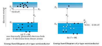
- Intrinsic Semiconductor: Pure semiconductors in which the electrical conductivity is totally governed by the electrons excited from the valence band to the conduction band and in which no impurity atoms are added to increase their conductivity are called intrinsic semiconductors and their conductivity is called intrinsic conductivity. Electrical conduction in pure semiconductors occurs by means of electron-hole pairs. In an intrinsic semiconductor-
ne = nh = ni
where ne = the free electron density in conduction band, nh = the hole density in valence band, and ni = the intrinsic carrier concentration. - Extrinsic Semiconductors: A Semiconductor doped with suitable impurity atoms so as to increase its conductivity is called an extrinsic semiconductor.
- Types of Extrinsic Semiconductors: Extrinsic semiconductors are of two types:
- n-type semiconductors
- p-type semiconductors
- n-type semiconductors: The pentavalent impurity atoms are called donors because they donate electrons to the host crystal and the semiconductor doped with donors is called n-type semiconductor. In n-type semiconductors, electrons are the majority charge carriers and holes are the minority charge carriers. Thus,
- p-type semiconductors: The trivalent impurity atoms are called acceptors because they create holes which can accept electrons from the nearby bonds. A semiconductor doped with acceptor type impurities is called a p-type semiconductor. In p-type semiconductor, holes are the majority carriers and electrons are the minority charge carriers Thus,
- Holes: The vacancy or absence of electron in the bond of a covalently bonded crystal is called a hole. A hole serves as a positive charge carrier.
- Mobility: The drift velocity acquired by a charge carrier in a unit electric field is called its electrical mobility and is denoted by
.
- The mobility of an electron in the conduction band is greater than that of the hole (or electron) in the valence band.
- Electrical conductivity of a Semiconductor:
- If a potential difference V is applied across a conductor of length L and area of cross-section A, then the total current I through it is given by-
where ne and nh are the electron and hole densities, and ve and vh are their drift velocities, respectively.
- If
and
are the electron and hole mobilities, then the conductivity of the semiconductor will be,
and the resistivity will be,
- The conductivity of an intrinsic semiconductor increases exponentially with temperature as,
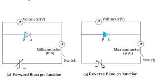
- Forward Biasing of a pn-junction: If the positive terminal of a battery is connected to the p-side and the negative terminal to the n-side, then the pn-junction is said to be forward biased. Both electrons and holes move towards the junction. A current, called forward current, flows across the junction. Thus a pn-junction offers a low resistance when it is forward biased.
- Reverse Biasing of a pn-junction: If the positive terminal of a battery is connected to the n-side and negative terminal to the p-side, then pn-junction is said to be reverse biased. The majority charge carriers move away from the junction. The potential barrier offers high resistance during the reverse bias. However, due to the minority charge carriers a small current, called reverse or leakage current flows in the opposite direction. Thus junction diode has almost a unidirectional flow of current.
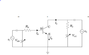
- Action of a transistor: When the emitter-base junction of an npn-transistor is forward biased, the electrons are pushed towards the base. As the base region is very thin and lightly doped, most of the electrons cross over to the reverse biased collector. Since few electrons and holes always recombine in the base region, so the collector current Ic is always slightly less then emitter current IE.
IE = IC + IB
Where IB is the base current
- Three Configurations of a Transistor: A transistor can be used in one of the following three configurations:-
- Common-base (CB) circuit
- Common-emitter (CE) circuit
- Common-collector (CC) circuit
- Current Gains of a Transistor: Usually low current gains are defined:-
- Common base current amplification factor or ac current gain
: It is the ratio of the small change in the collector current to the small change in the emitter current when the collector-base voltage is kept constant.
- Common emitter current amplification factor or ac current gain
: It is the ratio of the small change in the collector current to the small change in the base current when the collector emitter voltage is kept constant.
- Relations between
and
- Transistor as an amplifier: An amplifier is a circuit which is used for increasing the voltage, current or power of alternating form. A transistor can be used as an amplifier.
- AC Current Gain: AC current gain is defined as-
- DC Current Gain: DC current gain is defined as-
- Voltage Gain of an Amplifier: It is defined as-
i.e., Voltage gain = Current gain X Resistance gain.
- Power Gain of an Amplifier: It is defined as-
Logic Gate: A logic gate is a digital circuit that has one or more inputs but only one output. It follows a logical relationship between input and output voltage.
- Truth Table: This table shows all possible input combinations and the corresponding output for a logic gate.
- Boolean Expression: It is a shorthand method of describing the function of a logic gate in the form of an equation or an expression. It also relates all possible combination of the inputs of a logic gate to the corresponding output.
- Positive and Negative Logic: If in a system, the higher voltage level represents 1 and the lower voltage level represent 0, the system is called a positive logic. If the higher voltage represents 0 and the lower voltage level represents 1, then the system is called a negative logic.
- OR Gate: An OR gate can have any number of inputs but only one output. It gives higher output (1) if either input A or B or both are high (1), otherwise the output is low (0).
A + B = Y
Which is read as ‘A or B equals Y’.
- AND gate: An AND gate can have any number of inputs but only one output. It gives a high output (1) if inputs A and B are both high (1), or else the output is low (0). It is described by the Boolean expression-
A . B = Y
Which is read as ‘A and B equals Y’.
- NOT Gate: A NOT gate is the simplest gate, with one input and one output. It gives as high output (1) if the input A is low (0), and vice versa.
Whatever the input is, the NOT gate inverts it. It is described by the Boolean expression:
Which is read as ‘not A equals Y’.
- NAND (NOT + AND) gate: It is obtained by connecting the output of an AND gate to the input of a NOT gate. Its output is high if both inputs A and B are not high. If is described by the Boolean expression-
Which is read as ‘A AND B negated equals Y’.
- NOR (NOT + OR) Gate: It is obtained by connecting the output of an OR gate to the input of a NOT gate. Its output is high if neither input A nor input B is high. It is described by the Boolean expression.
Which is read as ‘A OR B negated equals Y’.
- XOR or Exclusive OR gate. The XOR gate gives a high output if either input A or B is high but not when both A and B are high or low. It can be obtained by using a combination of two NOT gates, two AND gates and one OR gate. It is described by Boolean expression:
The XOR gate is also known as difference gate because its output is high when the inputs are different.
- Integrated Circuits: The concept of fabricating an entire circuit (consisting of many passive components like R and C and active devices like diode and transistor) on a small single block (or chip) of a semiconductor has revolutionized the electronics technology. Such a circuit is known as Integrated Circuit (IC).
CBSE Class 12 Revision Notes and Key Points
Electronic Devices class 12 Notes. CBSE quick revision note for class-12 Physics, Chemistry, Math’s, Biology and other subject are very helpful to revise the whole syllabus during exam days. The revision notes covers all important formulas and concepts given in the chapter. Even if you wish to have an overview of a chapter, quick revision notes are here to do if for you. These notes will certainly save your time during stressful exam days.
- Physics
- Chemistry
- Mathematics
- Biology
- Accountancy
- Economics
- Business Studies
- Computer Science
- Informatics Practices
- English Core
- History
- Physical Education
To download Electronic Devices class 12 Notes, sample paper for class 12 Physics, Chemistry, Biology, History, Political Science, Economics, Geography, Computer Science, Home Science, Accountancy, Business Studies, and Home Science; do check myCBSEguide app or website. myCBSEguide provides sample papers with solution, test papers for chapter-wise practice, NCERT solutions, NCERT Exemplar solutions, quick revision notes for ready reference, CBSE guess papers and CBSE important question papers. Sample Paper all are made available through the best app for CBSE students and myCBSEguide website.
- Electric Charges and Fields class 12 Notes Physics
- Electrostatic Potential and Capacitance class 12 Notes Physics
- Current Electricity class 12 Notes Physics
- Moving Charges and Magnetism class 12 Notes Physics
- Magnetism and Matter class 12 Notes Physics
- Electromagnetic Induction class 12 Notes Physics
- Alternating Current class 12 Notes Physics
- Electromagnetic Waves class 12 Notes Physics
- Ray Optics and Optical class 12 Notes Physics
- Wave Optics class 12 Notes Physics
- Dual Nature of Radiation and Matter class 12 Notes Physics
- Atoms class 12 Notes Physics
- Nuclei class 12 Notes Physics
- Communication Systems class 12 Notes Physics
Test Generator
Create question paper PDF and online tests with your own name & logo in minutes.
Create Now
Learn8 App
Practice unlimited questions for Entrance tests & government job exams at ₹99 only
Install Now